Perovskite solar cells have long been considered a beacon of hope. But when scaling up, valuable percentages were usually lost. Researchers have now succeeded in reducing the loss of efficiency using tiny crystal seeds.
Researchers at the Qingdao Institute of Bioenergy and Bioprocess Technology (QIBEBT) of the Chinese Academy of Sciences recently published a new approach to perovskite solar cells. Using so-called CSV pre-seeding, they repaired microscopic defects on the hidden interfaces of the cells. The loss of efficiency when scaling to industrial dimensions was less than three percent and is lower than many previous reports.
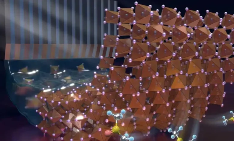
Inverted perovskite solar cells arrange the layers so that the hole transport layer lies beneath the light-absorbing material. To improve adhesion, the scientists modified the substrate with self-assembled monolayers (SAM). These layers often have a water-repellent effect, which usually makes uniform wetting with the liquid perovskite solution considerably more difficult.
Perovskite solar cells: Rod-shaped crystals as a guide
The researchers used specially developed, rod-shaped nanocrystals with the chemical formula PDPbI_4-DMSO for the process. This rod-shaped structure improves the spreading of the solution on the SAM surface and controls the growth of the perovskite layer. They act like signposts on a construction site where the crystals grow faster and more orderly.
When heated, the material releases the embedded dimethyl sulfoxide molecules (DMSO) in a controlled manner. This process of lattice-bonded solvent annealing creates a local gas zone directly at the interface. It acts like a protective haze under which the crystal grains arrange themselves stably and close defects in the material.
The researchers combined CSV pre-seeding with an industrial slot die coating to produce a mini-module with an area of 49.91 square centimeters. The device achieved an energy conversion efficiency of 23.15 percent. Compared to small laboratory cells, the efficiency fell by less than three percent, which exceeds many previous research reports.
New principle for semiconductor technology
The process closes cavities at the interface and ensures smoother transitions between the individual crystal grains. This creates a dense layer that is much more resistant to stress caused by light or heat. This technology overcomes the long-standing bottleneck in the mass production of high-performance perovskite modules.
Beyond photovoltaics, the concept establishes a versatile approach to other semiconductors. By specifically adapting organic cations, the chemical building blocks that determine the properties of the material, a broad library of CSV materials can be designed. This enables precise control of interfaces in various optoelectronic components.
The new principle opens doors for the development of more efficient light-emitting diodes (LEDs) or sensors based on soft-grid semiconductors. The strategy allows control over deep layers of material that were previously difficult to access. The discovery thus paves the way for industrial production of high-tech components that follows a similar principle to fast printing processes.
Also interesting:

Interest rate hit at NIBC!
Open yours now free NIBC daily money and receive up to 2.75 percent interest for your money – with daily availability!
Secure interest now
Requirements apply, advertisement